A little The SRF program currently consists of the Wafer Test Cavity, Polyhedral Cavity, and Isochronous Cyclotron (IC) Cavities. The Wafer Test Cavity was designed to serve as a short sample test cavity to evaluate the superconducting performance of materials and thin films. The first stage was the construction of the Dielectric Test Cavity to determine the low temperature properties of large single crystal sapphire. These test were completed at Jefferson National Lab in the fall of 2010. Currently the Wafer Test Cavity is being constructed at Jefferson Lab and the polyhedral is under construction at Bailey Tool and Manufacturing. It is expected that these cavities will be completed and initially tested in Fall of 2012. The IC cavities are currently under design for the ADS projects accelerating structures (see ADS for IC cavity).
Wafer Test Cavity
Polyhedral Cavity
The SRF program is developing a cavity to test the material properties of thin films at high magnetic field. The design of this cavity relies on a high purity single crystal of HEMEX sapphire. The dielectric acts as a lens focusing the fields on the 6 inch sample surface. The sapphire localize the field on the sample to 10 times higher values on the sample compared to the walls of the cavity. Thus the cavity is limited by the walls and the losses within the sapphire.
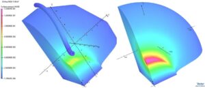
Dielectric Cavity shown below measured a 2 inch diameter, 6 inch tall single crystal (green) that provided a loss tangent of 5E-9. This measurement showed that we could measure on the order of 10s of nano- Ohms resistances. The crystal was not directly exposed to the liquid helium bath which is why in the Wafer Test cavity the sapphire was exposed directly. Sapphire is extremely conductive at these temperatures, thus should allow for lower error at higher magnetic fields. The anticipated frequency of the cavity was confirmed verifying others measurements of the dielectric constant tensor. The only problem this coupling was the asymmetry produced from the side port causing several complexities. 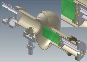
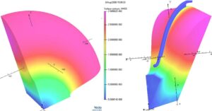
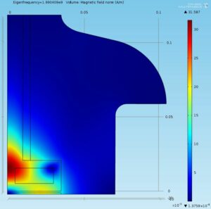
The Wafer Test Cavity was altered from its original design as a result of the data from the dielectric. The sapphire was heating faster than anticipated and thus the ratio of sample to cavity surface had to be increased. The reason the additional focusing was to reduce the amount of stored energy in the cavity, thus limiting the dissipation in the cavity. With a ratio of 10 to 1 the stored energy was reduced by a factor of 6.25 compared to the previous design, allowing for about an order of magnitude longer length of time to insert power to push to high field. The Wafer Cavity and its field distribution is shown below.
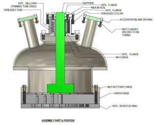
The goal of this cavity is to produce magnetic fields at or beyond the BCS limit of Niobium (230 mT) so that thin film heterostructures can be evaluated to their full potential. The Wafer Test cavity is funded by the Department of Energy and is in the process of final design and beginnings of construction.
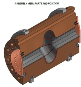
The polyhedral cavity is a superconducting cavity structure in which a multi-cell cavity is built from a Roman-arch assembly of arc segments. Each segment has a Tesla-like r-z profile, and is fabricated either by bonding a Nb foil to a Cu substrate wedge or by depositing a Nb surface on the Cu substrate. The segments are assembled with an arrangement of locking rings and alignment pins, with a controlled narrow gap between segments over much of the arc-span of adjoining segments. A tubular channel is machined in the mating surfaces of the Cu wedges. Dipole modes are suppressed by locating along each channel a tube coated with RF-terminating ferrite. A first model of the cavity is being built to investigate mode structure, evaluate alternatives for the Nb surface fabrication, and develop assembly. Show below is the single 3.9 GHz version that is currently being constructed. The multi-cell 1.3 GHz Telsa shape cavity is shown on the Home Page.
The areas marked in red indicate the Higher Order Mode (HOM) coupling channels. These channel have the possibility to remove the HOM modes that can deflect the beam due to imperfections. The HOM modes are harder to couple from cell to cell, thus increasing the iris diameter. If the HOM modes can be removed in cell, the iris can be reduced and therefore the gradient of the cavity can be increased substantially (factor of 1.7 possibly). The accelerating mode and leading deflecting mode is shown below.